Simple 10m CW Transmitter. Circuit Diagram.
The original circuit by the late Doug DeMaw W1FB, differs slightly from the one shown here. Two immediate differences are: A regulated DC supply for better frequency stability and a 2-pole low-pass filter for reduced harmonic output. The circuit is not as busy as first seems.
In fact, it’s just a permanent-running oscillator which is keyed either on or off before passing to the RF driver stage.
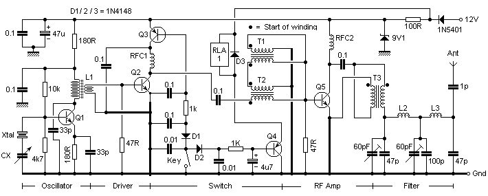
Q1 oscillator transistor is any NPN type with a high frequency transition. I used a BC182 and this works fine. In the original design a 50pF trimmer was placed across the collector and the 0.V rail but here I’ve used a fixed 33pF capacitor.
Capacitor ‘CX’ will pull the crystal approx. 5kHz of the fundamental frequency. As I only had a 28.0MHz crystal in the junk box, I used a 60pf trimmer mounted on the board to pull the frequency just above the band edge. Those of you who wish to vary the frequency could fix a 50pF air-spaced capacitor on the front panel of your chosen case. Otherwise, simply omit CX and use a wire link in place of.
Looking at L1, the primary is made up with 17 turns of 24 swg enamelled wire on a T50-6 toroid. Use the same gauge wire of three turns for the secondary which should be wound over the primary. It’s important to make sure here that both windings follow the same direction.
The oscillator runs continously to reduce ‘chirp’, but the signal is only apparent on Q2 (BFY51) output when turned on by Q3 (BC212) – key grounded to 0V. Output level at this stage is approx. 50mW.
The grounded key also triggers the antenna change-over relay via Q4 (another BC212). When the key is released, the 47uF capacitor holds the relay in for a short time delay. This prevents any ‘chatter’ on the contacts.
Our keyed oscillator signal now passes to the two transformers, T1 / T2. The easiest way to make these is using the following method:
Take two lengths of differing colour single-stranded wires (approx. 12inches long) and place one end of each length in the chuck of a hand drill. Fix the opposite ends in a vice. Keeping the wires taut, slowly turn the drill until you have a neat and uniform twist along the full length. All three transformers are identical so you’ll need to do this three times. As we’re using different coloured wires this makes it easier to locate the start windings for the correct phasing – get ’em wrong and the circuit won’t work!
When this is done carefully make seven complete turns on a FT-37-61 toroidal core. And that’s all there is to it!
The signal now enters the final RF driver, Q5 (BFY51 – I’d recommend a heatsink here). Now we should have a little over 1Watt on the output. For higher outputs replace Q5 with, for instance, a 2SC2166 (also with heatsink) and change the base resistor to a 10ohm 1Watt’er. (I’d also suggest by-passing the zener diode and 100ohm resistor for the full 12V input but since this is about QRP, I won’t!)
After T3 the signal enters a low-pass filter before reaching the antenna. Looking at the circuit you’ll see that this is simply two air-core inductors configured in a ‘PI’ network brought to resonance by their respective trimmers. Make these by winding 11turns of 18swg enamelled wire close-wound on an 8mm drill bit.
The two radio-frequency chokes, RFC1 / RFC2, are made up of 8turns each of 32swg enamelled wire on a ferrite bead.
When aligning the output, simply adjust the two 60pF trimmers for the highest signal. Some constructors may wish to add an identical 2-pole filter on the output for extra harmonic attenuation.
If you decide to construct this transmitter I’d suggest you start with the oscillator and work through until you reach inductor L1. When you get to here take your RF Diode Probe (seen elsewhere on these pages) and check your oscillator is working. Alternatively, a receiver with a digital display will check the precise frequency of your crystal/capacitor combination.
If there is no oscillation I’d suggest you check the wiring around inductor L1.
Next, add the components up to Q4. With your multi-meter, check you have the input voltage between Q4 Emitter and the +D.C rail when the key is grounded. If not, check the polarity of Diode D2. If all is well so far you can add the rest of the components. Finally, shove 12V D.C up the input and check you have roughly 9Volts on the ‘hot’ end of RFC2. Possible faults could be the 9V1 zener or the 1N5401 – check these are inserted with the correct polarity.
My transmitter was constructed ugly-style on a small matrix board. It’s quick, cheap and it works. A PCB is on the ‘to do’ list but I haven’t got around to the design just yet. If there’s any interest I’ll put the artwork on these pages.
Any small 12V relay will suffice for antenna change-over but it must have at least one set of SPDT contacts.


Last Comments